зҷ»еҪ•

- APP
дёӯеӣҪзІүдҪ“зҪ‘ж¬ўиҝҺжӮЁпј?/div>
- зІүдә«йҖҷь/a>
- 188188188b.comҪрұҰІ©
еҫ®дҝЎ

 е…іжіЁеҫ®дҝЎе…¬дј—еҸ¶ь/span>
- дёӯеӣҪзІүдҪ“зҪҗь/a>
 移еҠЁз«?/p>
 m.cnpowder.com.cn
зҷ»еҪ•
еҫ®дҝЎ
 е…іжіЁеҫ®дҝЎе…¬дј—еҸ¶ь/span>
![]() 移еҠЁз«?/p>
移еҠЁз«?/p>
 m.cnpowder.com.cn


еҸӮиҖғд»·ж »ь/p>йқўи®®
еһӢеҸ·
е“ҒзүҢ
дә§ең°
иӢұеӣҪж ·жң¬
жҡӮж—дјҡе‘ҳ
|з¬?е№іь/p>|
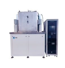
з”ҹдә§е•…ь/p>
![]() е·Ҙе•Ҷе·Іж ёе®қь/p>
е·Ҙе•Ҷе·Іж ёе®қь/p>
 з•ҷиЁҖиҜўд»·
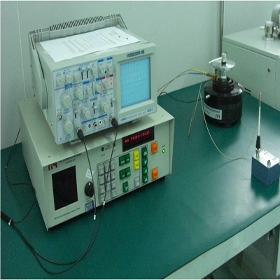
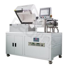
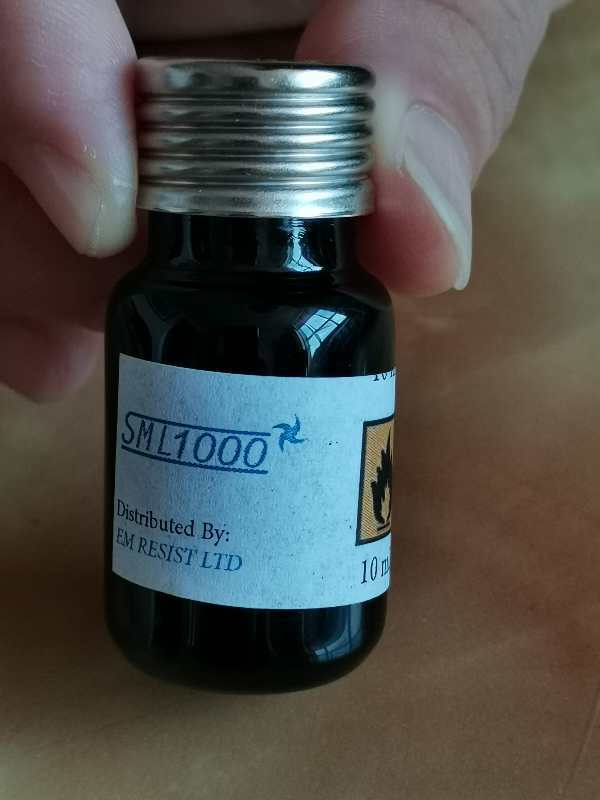
зңӢдәҶиӢұеӣҪEM SML Resistз”өеӯҗжқҹе…үеҲ»иғ¶зҡ„з”ЁжҲ·еҸҲзңӢдәҶ
з•ҷиЁҖиҜўд»·


иҷҡжӢҹеҸ·е°Ҷең180з§’еҗҺеӨұж•Ҳ
дҪҝз”Ёеҫ®дҝЎжү«з ҒжӢЁеҸ·
SML Resist вҖ Product Information
Introduction
The hardware of electron beam lithography has improved continuously over the past few decadesпјӢь/span>but electron beam resist technology has notпј and this is now one of the main limiting factors inimproved EBL performance.
The high performance SML resist is a novel polymer that has been specifically designed to answerthe demands of the EBL community. It can be simultaneously patterned into high resolution andhigh aspect ratio patternsпј even at low acceleration voltagesпј and without the aid of proximity effectcorrection.
Processing
Other Processing Information
гҖ Slow dry etch rate: significantly slowerthan PMMA
гҖ Can be hard-baked: Tg=109в„Ӯь/span>
гҖ Can be re-exposed after development
гҖ Other developers such as IPA:H2O canalso be used
гҖ Shelf life is guaranteed for 6 months
Products вҖ Spin Curves
How it Works - Monte Carlo Simulations
The following Monte Carlo simulations compare the electron scattering behaviour of PMMA andSML resists at 30KeV and at 100KeV. Each simulation contains 500 incident electrons and createdsecondary electrons are shown in light blue.
Comparison of 50nm thick PMMA & SML on Si substrate exposed @30keV
These simulations show that at both 30KeV and 100KeV:
гҖ The lateral scattering of incident electrons is much less in SML than in PMMA
гҖӮThe number of secondary electrons created is much less in SML than in PMMA
These properties mean that SML resist is less susceptible to the problem of proximity effect andenables the patterning of features with smaller critical dimensionsпј larger aspect ratioпј andstraighter side-wallsпј than those obtainable in PMMA resist.
About EM Resist Ltd
EM Resist Ltd specialises in electron beam lithography resists and applications. We develop andmanufacture electron beam resists in a purpose built cleanroom facility to ensure maximumquality and performance. We also have a dedicated team of applications scientists to aid ourcustomers with their questions and requirements.
Our products and expertise are the result of many years research by experienced physicists andmaterial scientists in both academia and industry. We are based in Macclesfieldпј UK and haveglobal sales and distribution channels for our products.
SML Resist вҖ Processing Information
Introduction
SML resist has been specifically designed for electron beam lithography. It is a polymer materialand can be processed in exactly the same way as other polymer resists such as PMMA or ZEP.
Storage
Do not refrigerate.
Store at room temperature.
Store away from direct sunlight and ignition sources.
The shelf life is guaranteed for six months.
Typical Processing Conditions
The processes outlined below are our standard processes. Other common resist processes canalso be used.
Substrate Preparation:
Solvent clean with Acetone and IPA.
SML has excellent adhesion to most substrates so HMDS is not generally required.
Spin Coating:
See spin curves below.
Baking:
Hot plate @ 180 C for 120-180 seconds.
Exposure:
Development:
MIBK:IPA (1:3) for 30 secondsпј followed by a rinse in IPA for 15 seconds.
Hard-Bake:
Convection oven @ 80 C for 30 minutes. (Tg=109в„Ӯьspan> )
Remover:
Acetone.
Spin Curves
Spin coater settings:
гҖӮRamp up time = 5 seconds.
гҖӮSpin time = 20 seconds.
гҖӮRamp down time = 10 seconds.
Safe Handling and Disposal
Caution: Flammable liquid.
Open in a well ventilated area.
Avoid inhalation.
Avoid direct contact with skin and eyes.
Wear appropriate safety equipment such as glasses and gloves.
In case of direct contact with eyesпј rinse thoroughly with water and seek medical advice.
Read the Material Safety Data Sheet.
Dispose of in appropriate waste containers for non-halogenated waste.
About EM Resist Ltd
EM Resist Ltd specialises in electron beam lithography resists and applications. We develop andmanufacture electron beam resists in a purpose built cleanroom facility to ensure maximum
quality and performance. We also have a dedicated team of applications scientists to aid our
customers with their questions and requirements.
Our products and expertise are the result of many years research by experienced physicists and
material scientists in both academia and industry. We are based in Macclesfieldпј UK and have
global sales and distribution channels for our products.
100 KeV Exposure Parameters
Please note that the best results (aspect ratio and resolution) are generallyachieved when a relatively low beam current is used.
100 KeV Exposure Parameters
30 KeV Exposure Parameters
25 KeV Exposure Parameters
SML Resist вҖ Contrast & Sensitivity
SML вҖ A Complete Solution for you вҖ Part 1 / 2
E M Resist can offer two complete solutions to suit your distribution needs in your territory.
SML вҖ A Complete Solution for you вҖ Part 2 / 2
жҡӮж— ж•°жҚ®пј
 иӢұеӣҪEM SML Resistз”өеӯҗжқҹе…үеҲ»иғ¶зҡ„е·ҘдҪңеҺҹзҗҶд»Ӣз»ҚпјҹиӢұеӣҪEM SML Resistз”өеӯҗжқҹе…үеҲ»иғ¶зҡ„дҪҝз”Ёж–№жі•пјҹиӢұеӣҪEM SML Resistз”өеӯҗжқҹе…үеҲ»иғ¶еӨҡе°‘й’ұдёҖеҸ°пјҹиӢұеӣҪEM SML Resistз”өеӯҗжқҹе…үеҲ»иғ¶дҪҝз”Ёзҡ„жіЁж„ҸдәӢйЎёь/li>иӢұеӣҪEM SML Resistз”өеӯҗжқҹе…үеҲ»иғ¶зҡ„иҜҙжҳҺд№Ұжңүеҗ—пјһь/li>иӢұеӣҪEM SML Resistз”өеӯҗжқҹе…үеҲ»иғ¶зҡ„ж“ҚдҪң规зЁӢжңүеҗ—пјҹиӢұеӣҪEM SML Resistз”өеӯҗжқҹе…үеҲ»иғ¶зҡ„жҠҘд»·еҗ«зҘЁеҗ«иҝҗиҙ№еҗ—пјҹиӢұеӣҪEM SML Resistз”өеӯҗжқҹе…үеҲ»иғ¶жңүзҺ°иҙ§еҗ—пјһь/li>иӢұеӣҪEM SML Resistз”өеӯҗжқҹе…үеҲ»иғ¶еҢ…е®үиЈ…еҗ—пјһь/li>
 жүӢжңәзүҲпјҡ